Thick coatings over 004 will tend to break sharp edges.
Resistance of a 3 micron thick sheet of copper.
If your target finished copper thickness is 1 oz we ll start with a oz sheet of material.
H hv gt 100 5 electric.
This is the standard starting copper thickness on the external layers for pcbs with the 3 oz finished copper weight selection.
And the anode positive electrode is usually either a block.
C1100 c1020 c1220 2 chemical composition c1100.
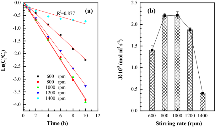
The table also shows the approximate resistance per square which is the edge to edge sheet resistance of any size square area of that weight of copper.
Because the production panels are completely covered with copper the excess copper needs to be removed to reveal your design.
Get an instant quote.
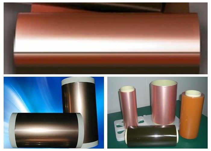
Our 25 micron thick copper foil is sourced from a reliable quality assured supplier in the united states.
Sheet resistance often called sheet resistivity is a measure of resistance of thin films that are nominally uniform in thickness.
The unit of measurement used to identify the thickness of a sheet of copper varies e g gauge mil ounces per square foot inches millimeters.
This is oz on each side.
It is commonly used to characterize materials made by semiconductor doping metal deposition resistive paste printing and glass coating examples of these processes are.
Other sunstone offers a variety of additional copper weights through a custom quote from 0 25 oz ft 2 to 6 oz and everything in between.
Doped semiconductor regions e g silicon or polysilicon and the resistors that are screen.
Thickness 002 to 0005 typical or as specified on drawing.
If your target finished copper thickness is 1 oz we ll start with a oz sheet of material.
If that trace is 1 2 ounce copper the dc resistance would be 1000 squares x 1 0.
To do this a 1 1 size image of your design is photo plotted onto a film.
Where extreme abrasion resistance is required do not seal as some softening will result.
The electrolyte is a solution of a salt of the metal to be coated.
This is oz on each side.
To do this a 1 1 size image of your design is photo plotted onto a film.
Electroplating is a general name for processes that create a metal coating on a solid substrate through the reduction of cations of that metal by means of a direct electric current the part to be coated acts as the cathode negative electrode of an electrolytic cell.
Because the production panels are completely covered with copper the excess copper needs to be removed to reveal your design.
Recommend seal hard anodize in 5 dichromate solution where increased corrosion resistance is required.
Corrosion resistance is good.
Below is a quick guide to help you determine which thickness best suits the needs of your project.
When specifying the thickness of copper on printed circuit boards pcbs the usual metric is ounces.
Copper sheeting comes in thicknesses ranging from very thin copper foil to thick copper plate.
As part of our commitment to delivering the highest quality graphene at affordable prices our in house substrate processing results in copper grain sizes that are tens of square centimeters in area.
O 1 4h 1 2h h o.